Digital Circuit Design (Part 2)
Part 1 of this post is a pre-req for this to make sense. Read it here for the required context.
Introduction
In the first part of this series I introduced the basics of digital circuit design by engineering a data path unit for computing simple moving averages. In this post, we’re going to wrap up the simple moving average module. I’ll start by introducing state machines and how we can leverage this abstraction to design a hardware control unit (CU) for the DPU we produced in part 1. Let’s dive into the fundamentals.
State Machines
In general, any system that utilizes state can be referred to as a state machine. The DPU from part 1 is technically a state machine under this definition. With a definition so broad, it’s likely unclear why this notion of a state machine is useful. The power of state machines as an abstraction becomes clear as the digital systems being designed become more complex. I really appreciate learning visually through diagrams, so let’s start there.
A state machine can be visualized using a flow chart referred to as a state diagram. Let’s look at a very simple state machine with three states:
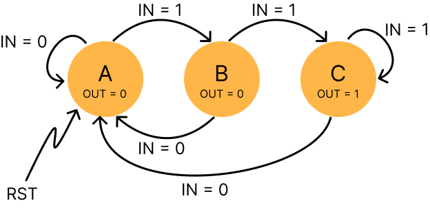
Circles or boxes generally represent different states (here we have states $A$, $B$, and $C$), while arrows represent state transitions. Arrow annotations (e.g. $IN = 1$) indicate which signals (conditions) cause a transition along that arrow. Output (control) signals are listed inside the state circle (e.g. $OUT = 0$). In other words, when in state $C$, the control signal OUT should be driven high. $RST$ indicates which state should be active on start (or reset) of the module.
Reading this diagram is now as simple as reading any other flow chart. On startup the system is in state $A$. While $IN = 0$, the state machine will remain in state $A$. If, on some future clock cycle, $IN = 1$, then a transition to state $B$ occurs, and so on.
You’ve likely realized by now that this state diagram will need to be implemented as a digital circuit. That is, we have to represent the components of this diagram using boolean algebra. Let’s try this for the inbound state transitions to $A$:
We should drive a state transition to $A$ if:
$$ (state = A \cdot IN = 0) + (state = B \cdot IN = 0) + (state = C \cdot IN = 0) + RST $$
Those familiar with boolean algebra can quickly derive a simplified expression:
$$ (IN = 0) + RST $$
The above expressions are the precursor to designing the Next State Logic. We’ll go deeper into that in the next section.
Diverging State Transitions
Before moving on, there are a couple important rules to keep in mind when designing state machines. The following rules apply for diverging state transitions (i.e. transitions out of the current state):
- All Inclusive Conditioning: Basically, at each clock tick we should transition somewhere (even if that transition is a self-loop). For a state with three diverging transitions with conditions $C_1$, $C_2$, and $C_3$, $C_1 + C_2 + C_3$ must be true. If it isn’t, then there’s some condition under which no transition occurs.
- No Mutual Exclusion Violations: Each pair of conditions taken together must be false. That is, $(C_1 \cdot C_2) + (C_2 \cdot C_3) + (C_1 \cdot C_3) = 0$. This ensures there exists no ambiguity in transitions. If $C_1$ and $C_2$ were both true, which path do you take?
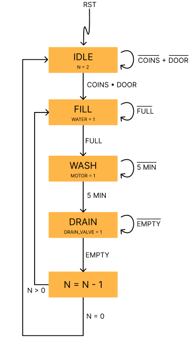
A Commonplace Example
Armed with this knowledge, let’s take a look at one more state machine using a real world device we’re all familiar with. Below is a state diagram for a coin-operated washer that runs two cycles. Try and run through the diagram yourself.
Simple Control Unit
Now that we understand state diagrams, let’s build a hardware control unit for the simple example introduced in the first section.
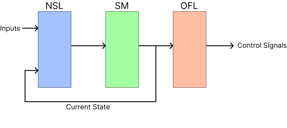
High-level Control Unit Architecture
The hardware control unit can be broken into three main blocks:
- Next State Logic (NSL): Combine the prevailing inputs and the current state to produce the next state.
- State Machine (SM): Memory elements to save the current state.
- Output Function Logic (OFL): Use current state to produce control signals (sent to DPU).
As a block diagram, the control unit looks like this:
State Machine (SM)
Let’s begin with the state machine. In this block, the current state must be encoded into a set of memory elements (flip flops). There’s two main approaches to this state encoding:
- Encoded State Assignment
- One-hot State Assignment
Encoded State Assignment
In this approach, the current state is encoded into a binary string. We have three states to encode, meaning we need two bits ($2^2 = 4$) to handle all possible states. Below is one possible encoding:

Where $Q_{S1}$ and $Q_{S2}$ represent the values of the flip flops. Keep in mind for the next section that this strategy requires two flip flops to encode the three states.
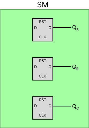
One-hot State Assignment
In contrast to encoded state assignment, using this strategy one flip flop is assigned to each state:

In this setup, one flip flop will always be “hot,” indicating the system is in that state. Recall that the encoded state assignment only required two flip flops. When designing a state machine, the memory requirements for each state assignment pattern must be considered. For certain designs, it might be easier to use one-hot state assignment, but the memory requirement grows linearly with the number of states. An encoded state assignment approach might be more complicated, but its memory requirement grows logarithmically with respect to states.
Implementation
For this simple example, I’m going to choose one-hot state assignment. The control unit has few states and the final circuit will be easier to understand for hardware beginners. The state machine block looks like this:
Now that state can be saved, it’s time to figure out how to set the state.
Next State Logic (NSL)
The NSL block is responsible for the combinational logic used to determine the next setting of the state machine block. This involves referencing the state diagram and converting the inbound transitions into digital logic. Recall the simplified expression for entering state $A$:
$$ (IN = 0) + RST $$
Let’s take a look at the state machine with the addition of next state logic:
Run through the NSL and convince yourself that each state is set appropriately. Are there any mutual exclusion violations? Are these conditions all inclusive? Notice that the NSL is informed by prevailing inputs as well as feedback from the current state.
Output Function Logic (OFL)
The last step in designing a complete control unit is determining how to generate control signals based on the current state. This circuit only has one control signal: $OUT$. In this case, the OFL is very simple. $OUT = 1$ IFF we’re in state $C$.
In other words, just connect $Q_C$ to $OUT$, because $OUT = 1$ only when $Q_C = 1$. This is now a completed control unit for the simple state machine example. Now it’s time to apply this process to the simple moving average module.
Simple Moving Average Control Unit
We are now tasked with designing a control unit that outputs the appropriate control signals for the SMA module’s DPU. At the end of part one we had the following DPU design:
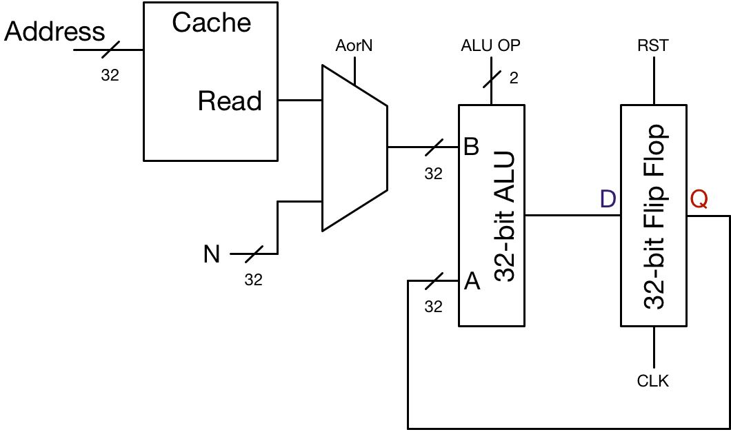
The corresponding state machine will have the following control signals:
- ALUOp: This tells the ALU which operation to perform. For this ALU, $0 \implies ADD$, $3 \implies DIV$. Remember that this line is two bits wide, meaning to send $0 \implies$ sending $00$, and to send $3 \implies$ sending $11$.
- AorN: This selects between the array value at the current address and the length of the array itself being supplied as input $B$ of the ALU.
- RST: This resets the flip flop to contain all zeros (we’re dealing with integers here so all data lines are 32 bits wide).
State Diagram
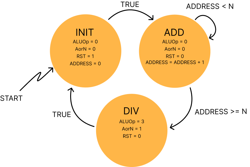
Running a single moving average computation requires three states: INIT, ADD, and DIV.
- INIT: Set the initial state of the system and reset memory to zero. Immediately move to ADD state on the next clock cycle.
- ADD: While the cache address $< N$ continue adding and increment the address1.
- DIV: Divide the accumulated amount by $N$. Immediately move to INIT state on next clock cycle2.
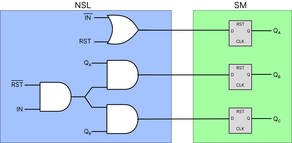
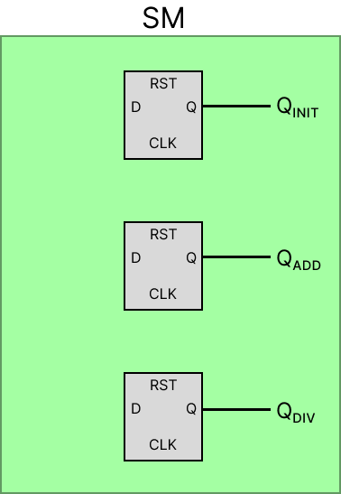
Now the hardware state machine can be easily implemented using a one-hot encoding scheme:
Now let’s add the next state logic:
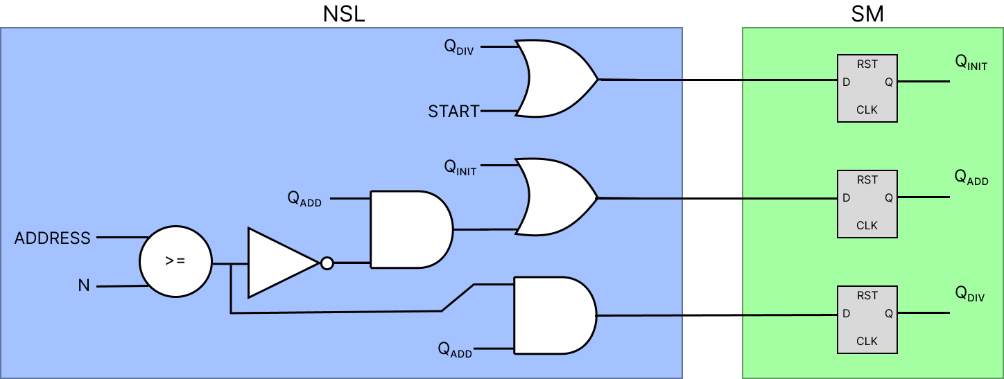
This time around, the next state logic is a bit more complex. Let’s break it down:
- Drive a transition to $Q_{INIT}$ if:
- Current state is $Q_{DIV}$ OR
- $START$ signal is on for one clock.
- Drive a transition to $Q_{ADD}$ if:
- Current state is $Q_{INIT}$ OR
- (current state is $Q_{ADD}$ AND Address is not $>= N$)
- Drive a transition to $Q_{DIV}$ IFF:
- Current state is $Q_{ADD}$ AND Address $>= N$
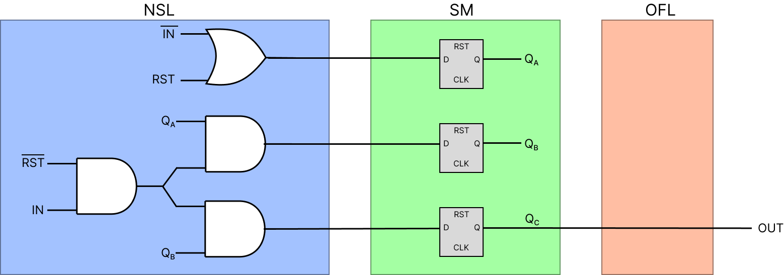
The last step is determining the output function logic. That is, how is information about the current state going to determine the control signals? Below is the final control unit with OFL:
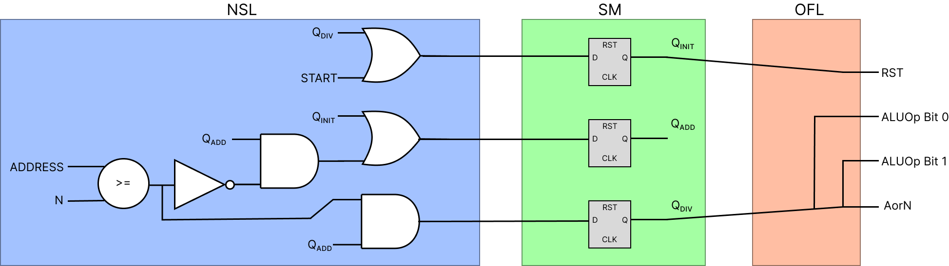
Here’s a summary of the OFL:
- $RST = Q_{INIT}$ because memory should only be reset in the $INIT$ state.
- $ALUOp$ bits are assigned to $Q_{DIV}$. Remember that $ALUOp$ is two bits wide. In the $ADD$ state, $Q_{DIV} = 00$ which means $ALUOp = 00$. In the $DIV$ state, $Q_{DIV} = 1$ which means $ALUOp = 11$ (base 2) $= 3$ (base 10)3.
- $AorN = 1$ only in the $DIV$ state. Thus, $AorN = Q_{DIV}$.
Conclusions
Let’s take a look at the DPU and CU side-by-side:
These two modules work together to form a circuit that computes moving averages. We’ve come a long way from the high-level code in Part 1:
function sma(A, n) {
  int sum = 0;
  for (int i = 0; i < n; i++) {
	sum += A[i];
  }

  return sum / n;
}
Fundamentally, these two implementations perform the same function. The former requiring no compiler or CPU cycle. Instead, the function is implemented directly in hardware.This implementation could gain some performance advantage over the software version, but this was a lot of work! Is it really worth it? This is the primary consideration when deciding to implement a function in hardware: does the performance advantage outweigh the effort required to both engineer and deploy? For many applications, the answer is yes!
Final Note on Deployment
Okay, now we have this hardware design… what do we do with it? There are two main paths one can travel to take this module into production: ASIC and FPGA.
- ASIC: Application Specific Integrated Circuit
- FPGA: Field Programmable Gate Array
An ASIC is an entirely new chip created for a specific purpose (application). This process is quite involved. ASICs require fabrication which can have turnaround times on the order of several months. The design has to be physically etched into the chip, thus any changes involve starting the fabrication process over. In this way, ASICs are not very flexible. However, they usually provide the greatest performance gains because unnecessary overhead can be eliminated (the circuit being etched is the design itself). FPGAs are the middle-ground solution between flexibility and performance. We’ll talk all about that in the next post.
-
For simplicity, we will assume that incrementing the address occurs for free in the background. In reality, this would also need to be a part of the design. ↩︎
-
The INIT state resets the flip flop to zero. In a real-world scenario, more than one clock cycle would be required to both divide and read the value (in order to actually do something with the result). ↩︎
-
There is an interesting lesson here about designing your circuit to interface with other components. Notice that, because this ALU happened to define an add operation as $00$ and a division operation as $11$, the OFL design was less complicated than if division was defined as $01$ (some extra gates would be required to convert $Q_{DIV}$ into $01$). ↩︎