Basics of the CPU Cycle
Introduction
Computers of all kinds have become central to our daily existence. The device you’re using to read this article is capable of performing billions of operations per second. There’s a lot that happens inside the CPU to run even a single operation. Let’s break it down.
For those of us familiar with high-level programming languages, writing some code to add two numbers is a fairly trivial task:
int a = 5;
int b = 10;
int c = a + b;
Add the value stored in
ato the value stored inband store that result in a new variable calledc.
High-level languages are great for humans, but the circuits inside your computer don’t understand int c = a + b. Your computer only understands information represented in binary, i.e. strings of 0 and 1.
It’s the job of the compiler to translate int c = a + b into a binary representation. How does a compiler work? Why does your computer only understand binary? Do some computers understand different physical languages? All great questions, and topics for future posts. For now, let’s take the first two questions for granted and move on.
Compilers (a brief sojourn)
I lied, we’re going to talk briefly about compilers, but only to further your understanding of the material. It turns out that taking human-readable code and converting it directly to something the CPU understands is hard. If you’re developing a compiler, you might want to take advantage of someone else’s labor. For example, some compilers might first convert the high-level code to a lower-level language like Assembly, then behind the scenes use the Assembly compiler1 to generate the binary representation. The programmer usually has no idea this is happening. The compiler looks and feels like a black box: code goes in, binary comes out.
Aside
Before we move on I need to define a term: “register.” You can think of registers as fast storage locations situated directly inside the CPU. They are used as placeholders for data the CPU wants to operate on. That is, if you want to run some kind of arithmetic operation, the data comes from the registers. This will be discussed in more detail later on.
Moving on, let’s take a look at some Assembly code keeping the previous example in mind. For int c = a + b, the compiler may generate something that looks like:
ADD $3, $1, $2
Add the value stored in register 1 to the value stored in register 2 and store the result in register 3
So, what’s the value in doing this intermediate step? Well, the keyword ADD is part of an instruction set. That is, for a given CPU architecture the assembler knows the translation between ADD and the appropriate CPU-interpretable binary representation. In fact, you can very nicely line up Assembly next to its binary representation to get an idea of how this works:
When all is said and done, the result is a binary representation of the operation:
10000 00001 00010 00011 00000 10000
While this looks like a random string of ones and zeros, there’s actually hidden meaning. Here’s how we can read that string (for ease of reading, I’ve also added the base 10 value of each section):
| OpCode | Read Reg 1 | Read Reg 2 | Write Reg | Shift | Function |
|---|---|---|---|---|---|
| 10000 | 00001 | 00010 | 00011 | 00000 | 10000 |
| 16 | 1 | 2 | 3 | 0 | 16 |
Okay, but what does that mean? Let’s look at each part individually:
- OpCode: This tells the CPU which operation it should perform. In this case we want to target the ALU (Arithmetic and Logic Unit).
- Read Reg 1: This is the first register we want to read from. It’s not a coincidence that the binary value corresponds directly with the register number in our assembly code.
- Read Reg 2: Second register to read from.
- Write Reg: The register where the result of our operation will be stored.
- Shift: This section is the “shift amount.” It’s used for operations requiring some kind of bit shift, but is not used here and we aren’t covering those types of operations in this article.
- Function: The last 5 bits represent the function. In this case, we want to
ADDtwo numbers.
End of the Line
Now that we’ve gone from
int c = a + b;
to
ADD $3, $1, $2
to
100000000100010000110000010000
this is where our software journey stops, and our hardware one begins. Your program is compiled and now you want to run it.
The CPU Cycle
To run your newly compiled program, your computer first loads the binary instructions into I-Cache (instruction cache). Once loaded, your CPU executes your instructions following the CPU Cycle.
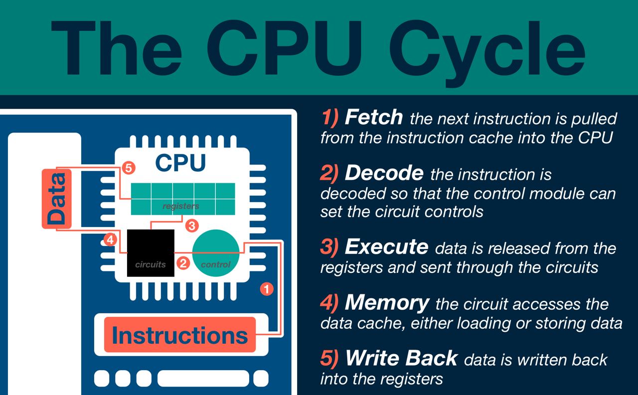
Fetch
Time to fetch! The next instruction to run is pulled from the instruction cache. Your CPU has an internal “program counter” used to keep track of the current “line” your program is on. If you recall from a previous section, that ADD instruction is simply a bit string. If we have many of those instructions in sequence (kinda like a software program) the result is just a list of bit strings!
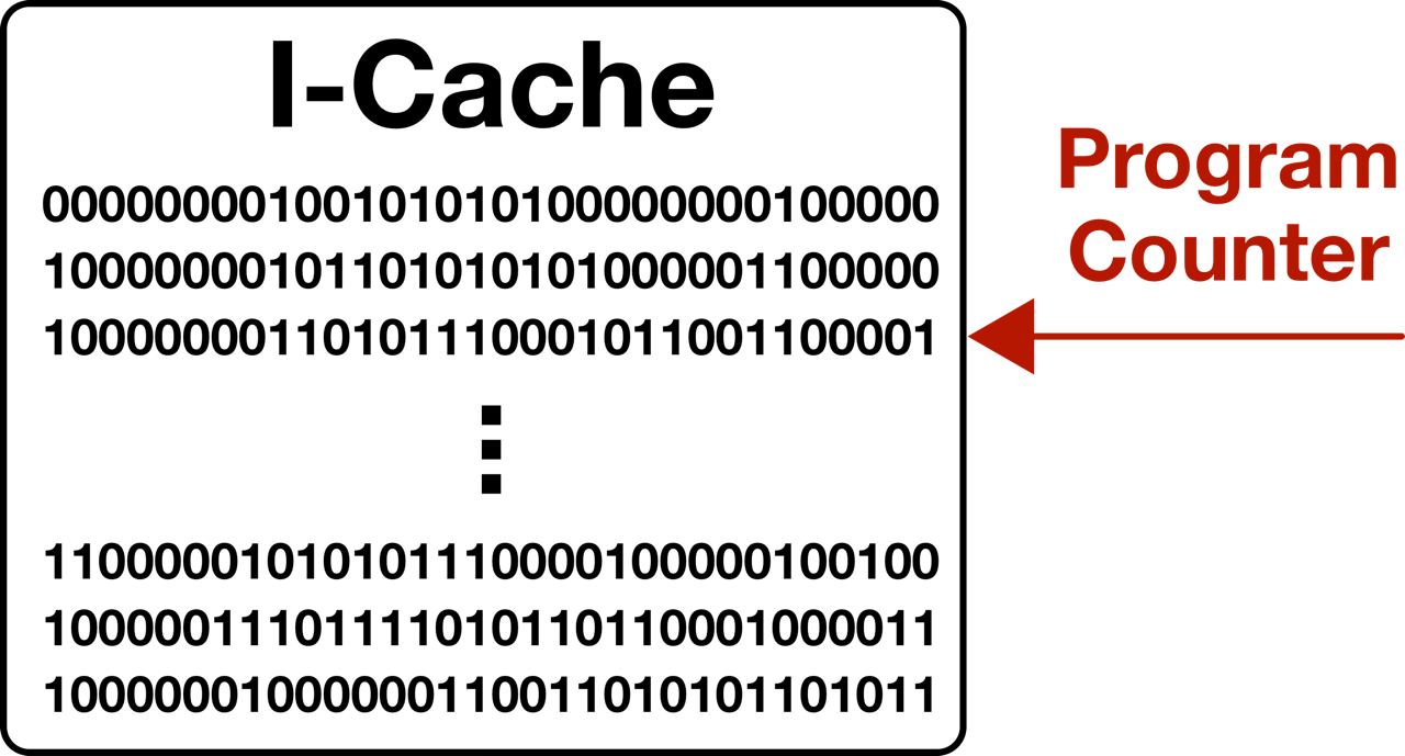
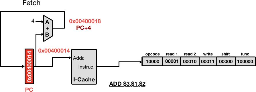
The output of the program counter is incremented to the next address and fed back into the PC register. The instruction at the address stored in PC is sent to the next stage to be decoded.
Decode
In the decode stage, the instruction cache output is broken down as described above. The OpCode and Function bits are fed to the control logic which in turn sets the appropriate downstream signals to run the specified operation.
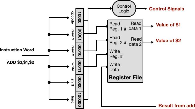
The Register File contains both the registers and the logic to read and write from them. It takes the register numbers as inputs, outputting the read data for the execute stage.
Execute
Time to crunch! The ALU performs the specified operation on the values from the register file, using the ALUop control signal to determine the function to run. This is where the addition actually takes place. We’ve instructed the register file to output the value of register 1 and 2, and write back the sum into register 3.
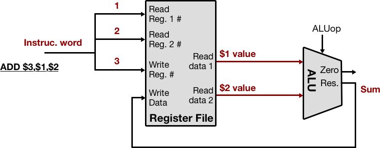
Conceptually, the write back step behaves as depicted above, but what if we have more data than fits in the registers? Registers are a very limited resource and data is constantly moving in and out to perform various operations. This begs the question, where do we store data in the interim?
Memory
Your computer has a few different ways to store data:
- non-volatile memory in the form of a hard disk or solid state drive
- volatile memory in the form of RAM (main memory), CPU cache, and registers
Volatile meaning memory that will lose data if power is interrupted. You might already be familiar with solid state drives and RAM, but there exists another layer inside the CPU itself (I’ve been alluding to it for a while). This memory location is referred to as cache. I-Cache (instruction cache) when we’re storing instructions, and D-Cache (data cache) when we’re storing data.
D-Cache provides an intermediary storage location between registers and main memory, reducing the cost of moving data in and out of registers. Let’s add some D-Cache into our diagram:
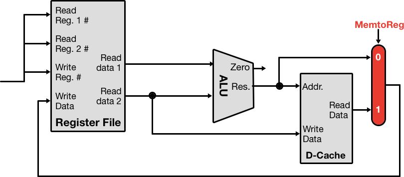
Notice that we now have a new hardware module sitting between the ALU and the Register File. The CPU now has the capability of moving data from the Register File to the D-Cache, using the ALU to compute the cache address. On the read side, data can be written back to the registers by appropriately setting the MemtoReg control signal.
Write Back
Finally, the write back stage determines which data to write back to the registers. Either we’ve performed some computation that we want to store (e.g. our ADD $3, $1, $2 operation), or we want to move data from D-Cache into the registers in order to perform some operation on that data.
Conclusions
That’s it (well, kinda… it’s never that simple)! Those are the basic steps involved in running an operation through a CPU. It’s worth mentioning that this is a extremely simplified version of the processor inside your laptop. I’ve skipped over a lot of details that are very important in modern CPU design including pipelining, out-of-order execution, cache coherency (just to name a few). Almost all CPUs, however, are based on this simple 5 step process.
-
The Assembly “compiler” is called the assembler and isn’t technically a compiler, there are some differences that aren’t important for the sake of this discussion. It’s also important to note that every compiler is different. Some compilers will translate directly from the high-level representation to machine code. ↩︎